Sale!

Germanium Wafer Customization

Customization Capabilities:

  • Custom Sizes and Thicknesses: We can produce Germanium wafers in a wide range of diameters and thicknesses to suit your specific application needs. From small-diameter wafers for specialized devices to large-diameter wafers for high-volume production, we ensure precision and consistency.
  • Doping and Resistivity: Tailor the electrical properties of your Germanium wafers with precise doping options. We offer both n-type and p-type doping with specific resistivity ranges to meet your device requirements.
  • Surface Finish: Achieve the desired optical and electrical performance with our high-quality surface finishes. Options include polished, lapped, and etched surfaces with low surface roughness and high flatness specifications.
  • Orientation: Choose from various crystallographic orientations such as <100>, <110>, and <111>, based on your application needs. Each orientation offers distinct advantages for different types of devices and processes.

Original price was: $100.00.Current price is: $50.00.

Description

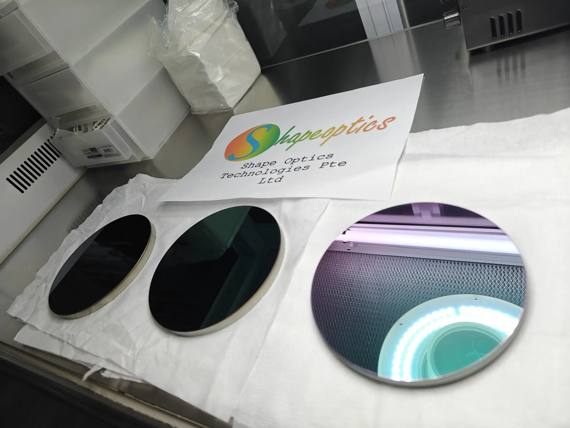
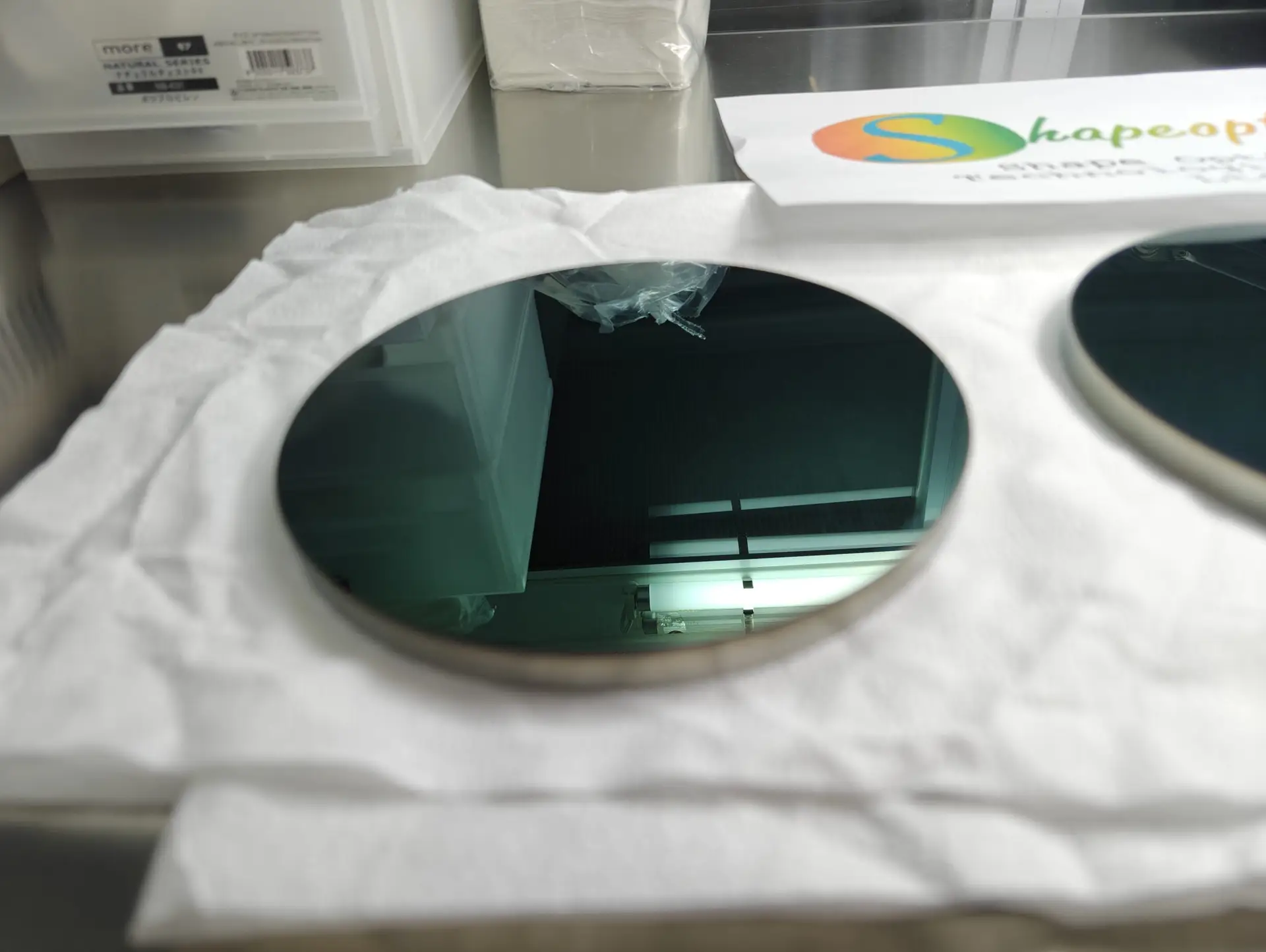
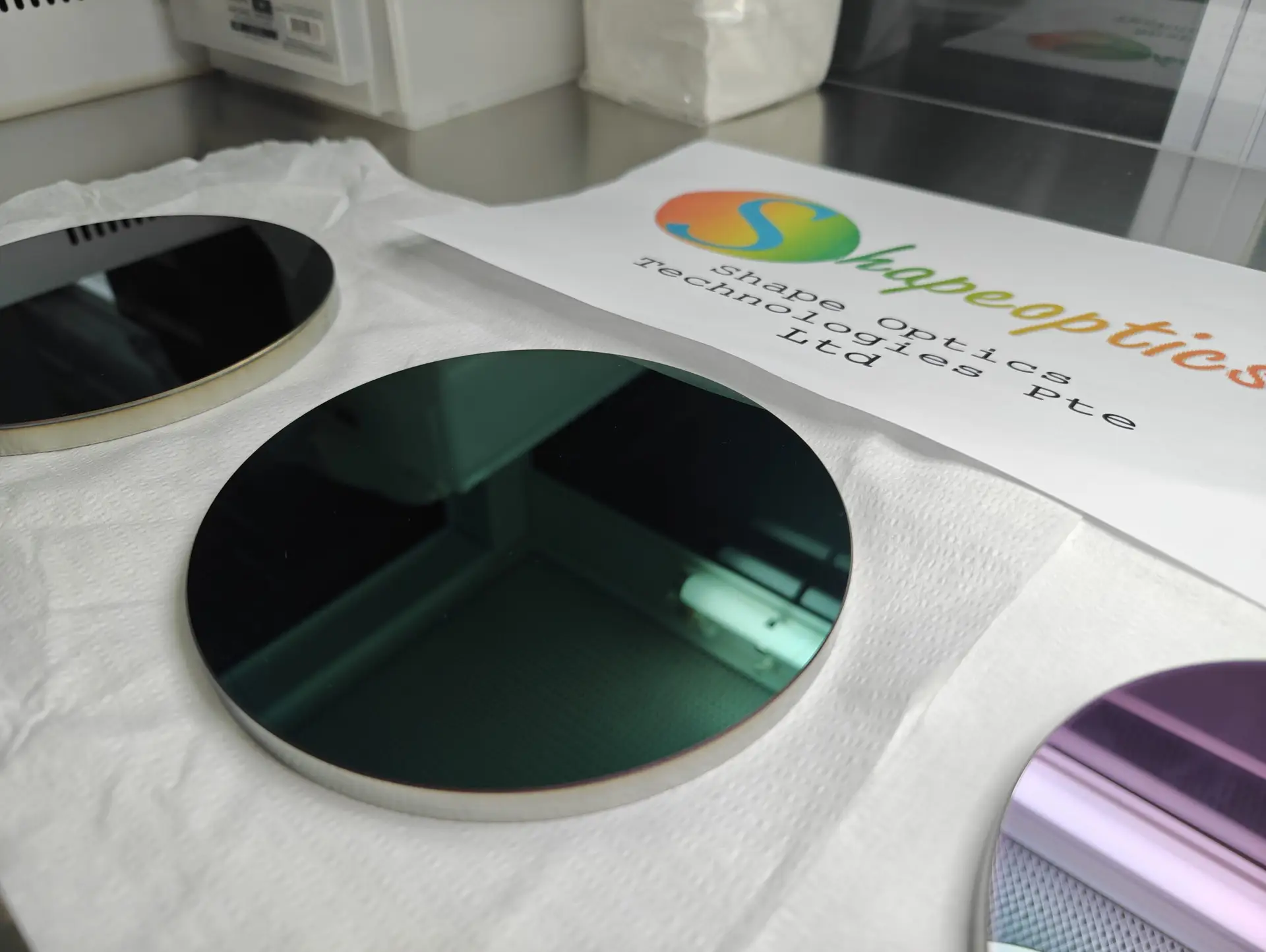
Welcome to our Germanium Wafer Customization service, where we specialize in providing high-quality, custom-fabricated Germanium wafers tailored to meet the unique requirements of various advanced applications. Our Germanium wafers are ideal for use in semiconductor, infrared, and photonics industries.

Key Products:

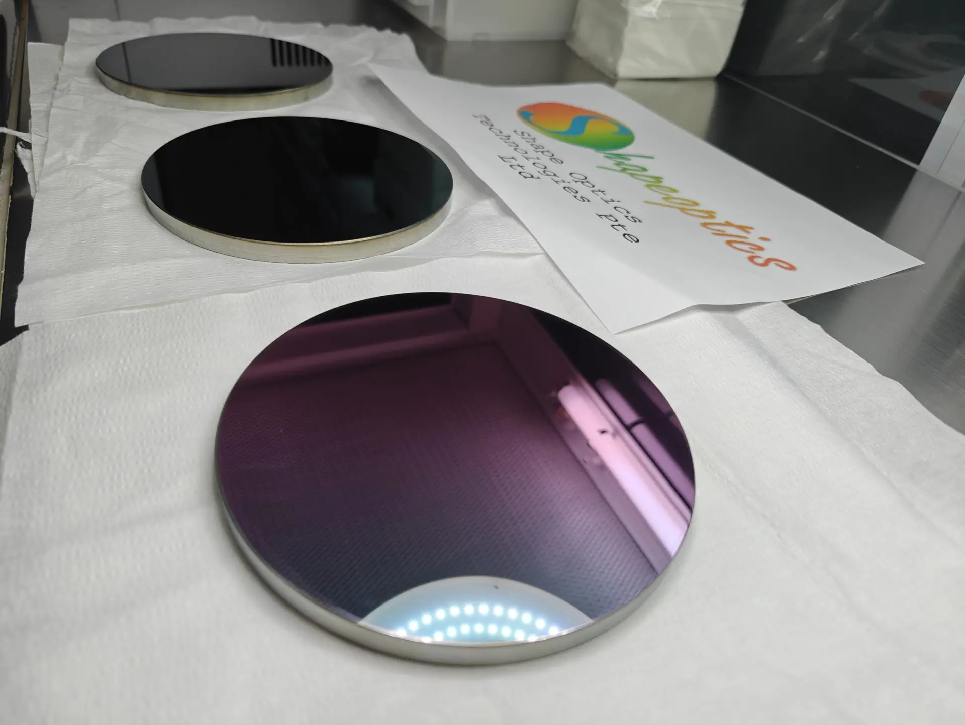
  • Semiconductor Wafers: Custom-doped Germanium wafers designed for semiconductor applications, providing excellent electronic properties and compatibility with silicon processes.
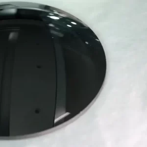
  • Infrared Wafers: High-purity Germanium wafers optimized for infrared applications, including thermal imaging, IR spectroscopy, and IR optics.
  • Photonics Wafers: Precision wafers for photonic devices, offering superior optical clarity and performance in photonic circuits and other light-based technologies.

Applications:

  • Semiconductor Devices: Germanium wafers are critical in the manufacture of high-speed transistors, diodes, and other semiconductor devices due to their excellent carrier mobility and compatibility with silicon.
  • Infrared Optics: Used in the production of IR detectors, lenses, and windows, Germanium wafers provide high transmittance in the infrared spectrum.
  • Photonics: Essential for photonic integrated circuits and other photonic devices that require precise control over light propagation and interaction.
  • Research and Development: Ideal for experimental and prototyping applications in academic and industrial research settings.

Why Choose Our Germanium Wafer Customization Service?

  • Expertise: Our team of engineers and material scientists has extensive experience in the design and fabrication of custom Germanium wafers.
  • Quality Assurance: We adhere to strict quality control standards, ensuring that every wafer meets or exceeds industry specifications.
  • Advanced Technology: We utilize state-of-the-art equipment and processes to deliver high-precision and high-quality wafers.
  • Customer-Centric Approach: We collaborate closely with our clients to understand their specific needs and provide tailored solutions that deliver superior performance.

Ordering Process:

  1. Consultation: Contact us to discuss your specific requirements and project details.
  2. Design and Prototyping: Our engineers will design your custom Germanium wafers using advanced modeling software and create prototypes for evaluation.
  3. Manufacturing: Once the design is approved, we will manufacture the wafers using our high-precision equipment.
  4. Quality Inspection: Each wafer undergoes rigorous quality inspection to ensure it meets your specifications.
  5. Delivery: We will ship your custom Germanium wafers, ensuring they arrive safely and on time.

Contact Us: To learn more about our Germanium customization services or to start your project, please contact us at:

Experience the excellence of customized Germanium wafers with Shape Optics, where precision meets performance.

Additional information

Weight 1 kg
Dimensions 12 × 10 × 8 cm

Reviews

There are no reviews yet.

Be the first to review “Germanium Wafer Customization”

Your email address will not be published. Required fields are marked *

General Specification
  • Material: Optical-Grade Monocrystalline Germanium ( resistivity of 5-40 ohm cm)
  • Diameter: Ranges from 12mm to 380mm
  • Length: Customizable
  • Electrical Resistivity: From 0.005Ω to 50Ω/cm
  • Crystal Purity: Between 99.999% and 99.9999%
  • Surface Roughness: From Ramax 0.2μm to 4.0μm
  • Refractive Index at 10.6μm: 4.0052
  • Absorbance at 10.6μm: ≤0.035
  • Thickness Tolerance: ± 0.10mm
  • Diameter Tolerance: +0.00/-0.05mm
  • Edge Finish: Finely ground
  • Surface Quality: 60/40 Scratch/Dig
  • Surface Flatness: ≤ 5 Fringes at 633nm
  • Parallelism: ≤ 3 Arc minutes
  • Orientation: <111>
  • Transmission Range: Covers IR wavelengths from 3 to 14 microns
  • Coating Specification: Upon Request, Anti-Reflective/Diamond-Like Carbon (AR/DLC)
  • Coating: AR coated from 3-14 microns, or DLC (Diamond-Like Carbon) in black/dark grey colour, with average transparency (Tavg) greater than 80%
  • Double-sided Anti-Reflective coating with an average transparency (Tavg) greater than 85%
A graph with a line drawn on it Description automatically generated

Here is the clearer plot of the typical transmission curve for a 1mm thick Germanium (mono-crystalline) window. The graph shows a sharp increase to 50% transmission starting from 2 µm and remains constant through 16 µm. This graph provides a visual representation of how the transmission behaves across the specified wavelength range.

Germanium Physical Properties

This table details various physical properties of the material, which could include mechanical, thermal, and electrical characteristics, relevant for applications that require precise material specifications.

the refractive index of a material Germanium

This table provides the refractive index of a material over the wavelength range from 2 micrometres to 14 micrometres, useful for applications requiring optical properties data at different IR spectrums.

optical characteristics of Germanium

This table presents various optical characteristics, including transmission spectrum, refractive index, and optical transmittance, which are crucial for understanding the performance of optical materials in specific applications, especially those involving precise wavelength requirements.

Shape Optics Diamond-Like Carbon (DLC) Coated Germanium Windows are crafted for robustness and longevity. These windows are equipped with a high-efficiency broadband anti-reflection coating on one side and a durable DLC coating on the opposite side, ensuring outstanding transmission and resistance to environmental conditions. The DLC-coated surface is engineered to endure extreme temperature fluctuations ranging from -80 to +160°F, continuous exposure to salt spray for 24 hours, salt solubility during a 24-hour immersion, and up to 5,000 wiper oscillations with a sand and slurry mixture. Moreover, ShapeOptics DLC Coated Germanium Windows comply with the MIL-C-675C standards for severe abrasion resistance.

Shape Optics offers Germanium (Ge) Windows with three options for anti-reflection coatings to cater to different infrared (IR) applications: a 3 – 5μm coating for mid-infrared use, a 3 – 12μm coating for broadband multispectral applications, and an 8 – 12μm coating for thermal imaging systems. Given germanium’s high index of refraction, approximately 4.0 across the 2 – 14μm wavelength range, applying an anti-reflection coating is crucial for achieving adequate transmission within the desired spectral region.

3 - 5μm coating for mid-infrared of Germanium

Typical transmission of a 3mm thick Ge window with BBAR (3000-5000nm) coating at 0° AOI. It indicates the coating design wavelength range, with the following specification: Ravg <3% @ 3000 - 5000nm

3mm thick Ge window

Typical transmission of a 3mm thick Ge window with BBAR (3000-12000nm) coating at 0° AOI. It indicates the coating design wavelength range, with the following specification: Ravg <5.0% @ 3 - 12μm

3mm thick Ge window with BBAR (8000-12000nm)

Typical transmission of a 3mm thick Ge window with BBAR (8000-12000nm) coating at 0° AOI. It indicates the coating design wavelength range, with the following specification: Ravg <3.0% @ 8 - 12μm

Germanium is prone to thermal runaway, a condition where its transmission efficiency declines as temperatures rise. Therefore, it is recommended to operate Shape Optics Germanium Windows at temperatures below 100°C to maintain optimal performance. Additionally, with a high density of 5.33 g/cm³, germanium windows should be carefully integrated into designs where weight sensitivity is a factor.

The material’s Knoop Hardness, at 780, is roughly double that of magnesium fluoride, making germanium windows exceptionally suitable for demanding IR applications where durable optics are essential.

  • Adhesion Test Compliant with MIL-C-675C military standards, an adhesion test involved applying a tape that meets LT-90 specifications onto the lens film layer. The tape was affixed fully and then removed vertically. This procedure was performed three times, resulting in no blistering or peeling.
  • Temperature Test In line with MIL-C-675C specifications, test pieces were subjected to temperatures of -62±1℃ and 71±1℃. After maintaining them at room temperature (16℃~32℃) for two hours, the adhesion test was repeated, confirming no film detachment.
  • Abrasion Resistance Test Conforming to MIL-C-675C and CCC-C-440 standards, the abrasion resistance test involved a gauze tester applying a minimum force of 1.0 lbs (0.45 kg) to the film. This was repeated 25 times with gauze widths of 1/4 inch (6.4mm) and 3/8 inch (9.5mm), ensuring no damage occurred to the film surface.
  • Humidity Test Under MIL-C-675C criteria, the test piece was placed in a controlled temperature and humidity chamber set to 49 ±2℃ and 95%~100% humidity for 24 hours. The film remained intact, with no peeling, scratches, or other defects.
  • Solvent and Cleaning Testing Following MIL-C-675C specifications, test pieces were exposed to room temperature conditions (16℃~32℃) and tested with acetone and alcohol for at least 10 minutes each. After air drying and subsequent cleaning with a cotton cloth soaked in alcohol, the film surface showed no signs of peeling or scratches.
  • Salt Spray Test After 100 hours in a 35°C environment with a 5% saltwater concentration, the film showed no signs of damage.

Polycrystalline Germanium:

  • Structure: Made up of many small crystalline grains or crystals, each with a different orientation.
  • Production: Easier and cheaper to produce compared to monocrystalline germanium.
  • Efficiency: Generally less efficient in electronic and photovoltaic applications because grain boundaries can scatter charge carriers, reducing their mobility.
  • Applications: Often used in less demanding electronic applications, such as infrared optics, and in some solar cells.

Monocrystalline Germanium:

  • Structure: Consists of a single, continuous crystal lattice with no grain boundaries.
  • Production: More difficult and expensive to produce as it requires precise control of the crystal growth process.
  • Efficiency: Higher efficiency in electronic and photovoltaic applications due to fewer defects and better charge carrier mobility.
  • Applications: Preferred for high-performance applications, such as in high-speed transistors, and high-efficiency solar cells.
P-Type Polycrystalline Germanium Window 11
P-Type Polycrystalline Germanium Window 16

N-type Germanium:

  • Doping: Doped with elements that have more valence electrons than germanium (group V elements like phosphorus, arsenic, or antimony).
  • Charge Carriers: The majority charge carriers are electrons.
  • Behavior: When an electric field is applied, electrons move towards the positive terminal, making it a negative type (N-type) semiconductor.
  • Applications: Used in various electronic components, including diodes, transistors, and integrated circuits.

P-type Germanium:

  • Doping: Doped with elements that have fewer valence electrons than germanium (group III elements like boron, gallium, or indium).
  • Charge Carriers: The majority charge carriers are holes (the absence of an electron).
  • Behavior: When an electric field is applied, holes move towards the negative terminal, making it a positive type (P-type) semiconductor.
  • Applications: Also used in electronic components, often in conjunction with N-type materials to create P-N junctions, which are essential for diodes, transistors, and solar cells.
  • Comparison of P-type and N-type Semiconductors:

    FeatureP-typeN-type
    Dopant ElementsBoron, Gallium, IndiumPhosphorus, Arsenic, Antimony
    Majority Charge CarriersHolesElectrons
    Direction of Current FlowHoles move to negative terminalElectrons move to positive terminal