Description
P-type germanium is a semiconductor material formed by doping germanium with acceptor impurities that create an excess of holes, which act as the majority charge carriers. This controlled doping modifies the electrical behavior of germanium while largely preserving its fundamental material properties.
Doping Elements
P-type germanium is typically doped with group III elements, including:
- Boron
- Gallium
- Indium
These dopants have fewer valence electrons than germanium. When introduced into the germanium lattice, they create electron vacancies—known as holes—which behave as positive charge carriers.
Electrical Properties
- Majority Charge Carriers: Holes
- Electrical Conductivity: Governed by hole movement through the crystal lattice
- Carrier Motion: Under an applied electric field, holes drift toward the negative terminal (cathode)
- Conventional Current: Flows from the positive terminal to the negative terminal, in the same direction as hole motion
P-type germanium exhibits high hole mobility, contributing to efficient charge transport in semiconductor devices.
Uses in Technology
- Semiconductor Devices
- Transistors: Historically used in bipolar junction transistors (BJTs) and other discrete semiconductor devices
- Integrated Circuits: Applied in complementary structures with N-type material, forming P–N junctions essential for diodes, transistors, and other semiconductor components
- Detectors: Used in certain radiation and infrared detector technologies
- Optical Applications
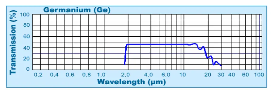
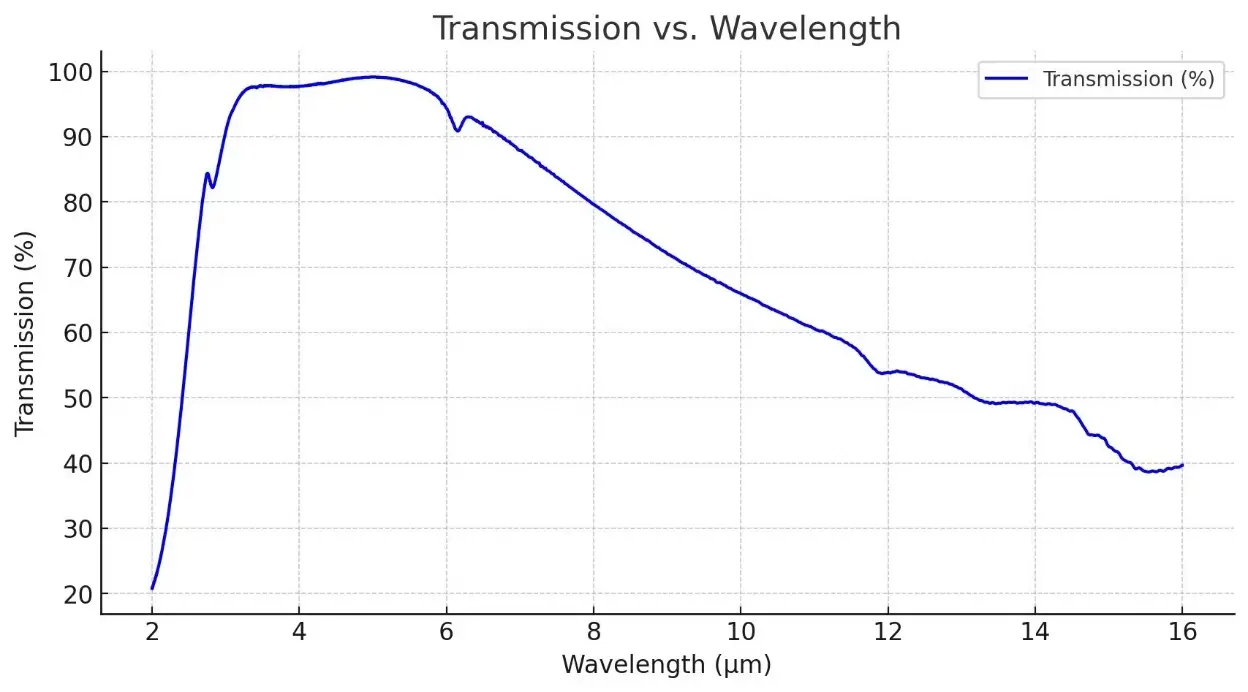
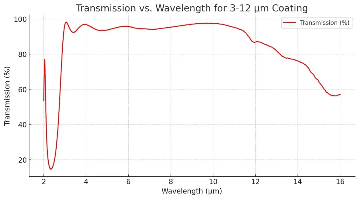
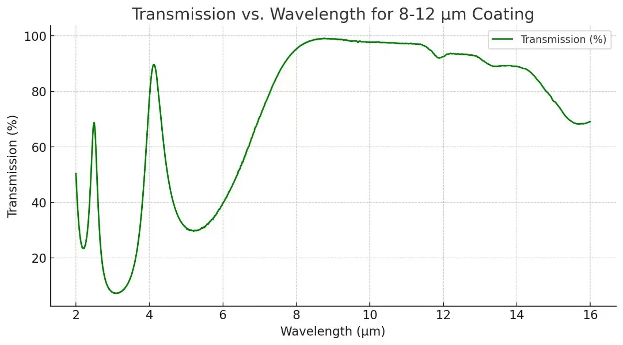
- Infrared Optics: P-type germanium is widely used as a substrate material for infrared lenses and windows, especially where high resistivity is required to minimize free-carrier absorption
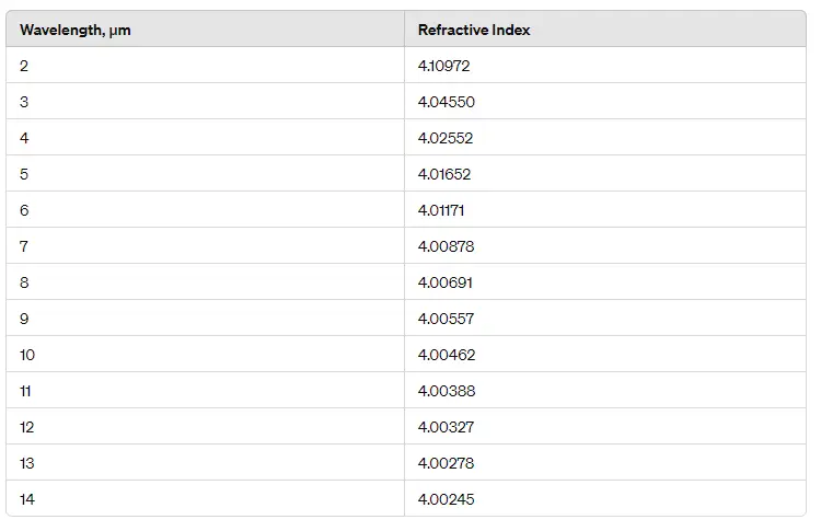
- Optical Coatings: Germanium itself is not an anti-reflective coating material. Instead, it may be used as a high-refractive-index thin-film layer within certain infrared coating stacks
- Optical Storage Media: CDs, DVDs, and Blu-ray discs do not use pure P-type germanium films. These media rely on phase-change alloys (such as Ge–Sb–Te), where germanium is only one component of a compound material
Advantages
- Essential for P–N Junctions: Enables diodes, transistors, and integrated semiconductor devices
- High Hole Mobility: Higher than silicon, supporting faster device operation in specific applications
- Infrared Compatibility: Well suited for infrared detectors and optical systems when properly specified
Note: Due to germanium’s relatively narrow bandgap, P-type germanium—like N-type—is less suitable for high-temperature or high-power electronics than silicon.
Comparison to Silicon
- Similarities:
- Both are group IV semiconductors
- Both can be doped to form P-type and N-type materials
- Used in electronic and optoelectronic devices
- Differences
- Hole Mobility: Germanium > Silicon
- Bandgap: Germanium has a smaller bandgap, resulting in higher leakage currents
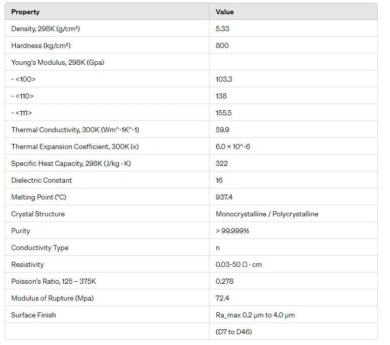
- Thermal Stability: Germanium melts at ~937°C, lower than silicon (~1414°C)
- Modern Usage: Silicon dominates mainstream electronics; germanium is used mainly in high-speed, infrared, and specialized semiconductor applications
Summary
P-type germanium is a key semiconductor material whose electrical properties are tailored through acceptor doping to create holes as the majority carriers. It is indispensable for forming P–N junctions and remains highly relevant in infrared detectors, optoelectronics, and specialized semiconductor devices. While no longer common in mainstream IC manufacturing, P-type germanium continues to play an important role where high carrier mobility and infrared compatibility are required.


