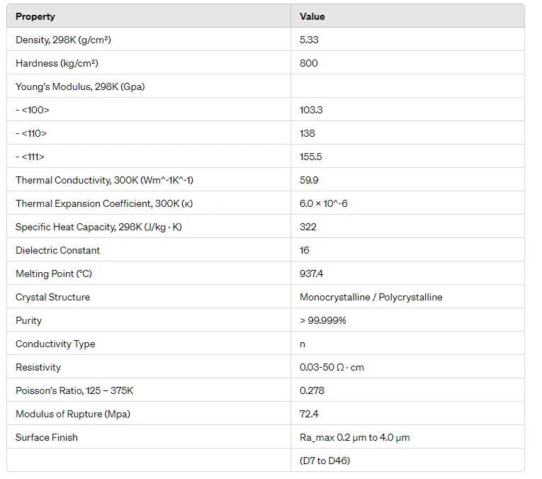
Monocrystalline Germanium P Type Crystal AR Coated & DLC Coated, Ge Window

Germanium windows deliver excellent infrared transmission across the 2–14 µm wavelength range, making them well suited for both mid-wave (MWIR) and long-wave infrared (LWIR) systems. As one of the most commonly used materials for IR windows and lenses, germanium is a core component in thermal imaging and infrared sensing technologies, valued for its high refractive index and strong infrared performance.

As a high-density infrared material, germanium exhibits temperature-dependent transmission behavior—often referred to as thermal escape—where increasing window temperature leads to higher absorption and reduced transmission efficiency. Despite this characteristic, germanium windows are widely adopted across defense and aerospace, life and medical sciences, and industrial OEM applications, as well as many other systems that require reliable and high-performance infrared functionality.

Price range: $198.00 through $1,292.43

$198.00
$209.01
$415.77
$415.77
$730.80
$1,292.43
$198.00
$209.01
$415.77
$415.77
$730.80
$1,292.43
$198.00
$209.01
$415.77
$415.77
$730.80
$1,292.43

Important Remark

The minimum cart order value is USD 2,000. Stock and lead time are subject to confirmation, and listed prices are for reference only—please email us to confirm availability and final pricing before ordering.

Description

P-type germanium is a semiconductor material formed by doping germanium with acceptor impurities that create an excess of holes, which act as the majority charge carriers. This controlled doping modifies the electrical behavior of germanium while largely preserving its fundamental material properties.


Doping Elements

P-type germanium is typically doped with group III elements, including:

  • Boron
  • Gallium
  • Indium

These dopants have fewer valence electrons than germanium. When introduced into the germanium lattice, they create electron vacancies—known as holes—which behave as positive charge carriers.


Electrical Properties

  • Majority Charge Carriers: Holes
  • Electrical Conductivity: Governed by hole movement through the crystal lattice
  • Carrier Motion: Under an applied electric field, holes drift toward the negative terminal (cathode)
  • Conventional Current: Flows from the positive terminal to the negative terminal, in the same direction as hole motion

P-type germanium exhibits high hole mobility, contributing to efficient charge transport in semiconductor devices.


Uses in Technology

  • Semiconductor Devices
    • Transistors: Historically used in bipolar junction transistors (BJTs) and other discrete semiconductor devices
    • Integrated Circuits: Applied in complementary structures with N-type material, forming P–N junctions essential for diodes, transistors, and other semiconductor components
    • Detectors: Used in certain radiation and infrared detector technologies
  • Optical Applications
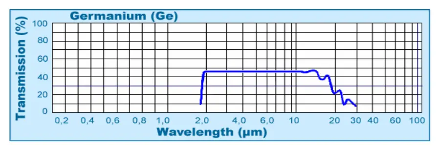
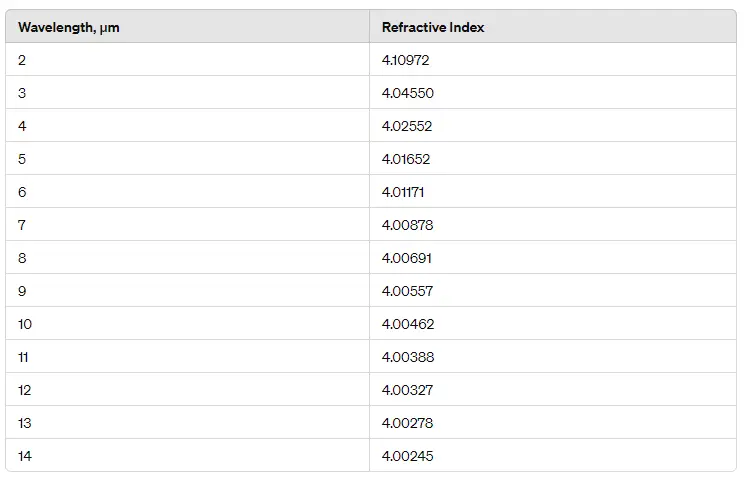
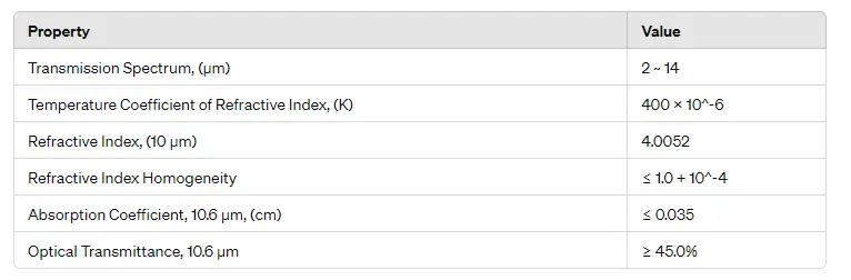
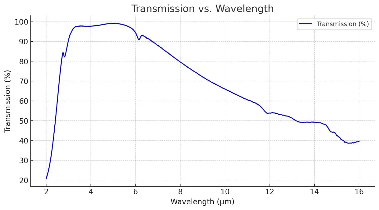
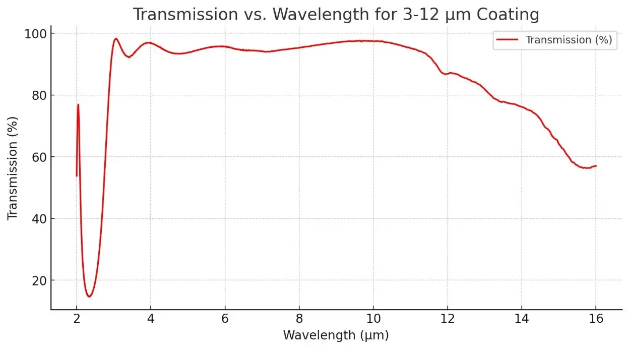
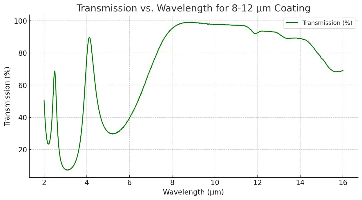
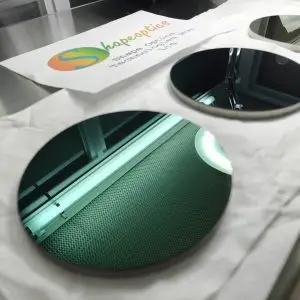
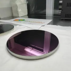
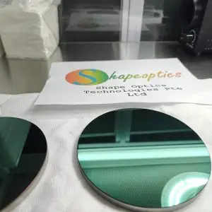
    • Infrared Optics: P-type germanium is widely used as a substrate material for infrared lenses and windows, especially where high resistivity is required to minimize free-carrier absorption
    • Optical Coatings: Germanium itself is not an anti-reflective coating material. Instead, it may be used as a high-refractive-index thin-film layer within certain infrared coating stacks
    • Optical Storage Media: CDs, DVDs, and Blu-ray discs do not use pure P-type germanium films. These media rely on phase-change alloys (such as Ge–Sb–Te), where germanium is only one component of a compound material


Advantages

  • Essential for P–N Junctions: Enables diodes, transistors, and integrated semiconductor devices
  • High Hole Mobility: Higher than silicon, supporting faster device operation in specific applications
  • Infrared Compatibility: Well suited for infrared detectors and optical systems when properly specified

Note: Due to germanium’s relatively narrow bandgap, P-type germanium—like N-type—is less suitable for high-temperature or high-power electronics than silicon.


Comparison to Silicon

  • Similarities:
    • Both are group IV semiconductors
    • Both can be doped to form P-type and N-type materials
    • Used in electronic and optoelectronic devices
  • Differences
    • Hole Mobility: Germanium > Silicon
    • Bandgap: Germanium has a smaller bandgap, resulting in higher leakage currents
    • Thermal Stability: Germanium melts at ~937°C, lower than silicon (~1414°C)
    • Modern Usage: Silicon dominates mainstream electronics; germanium is used mainly in high-speed, infrared, and specialized semiconductor applications


Summary

P-type germanium is a key semiconductor material whose electrical properties are tailored through acceptor doping to create holes as the majority carriers. It is indispensable for forming P–N junctions and remains highly relevant in infrared detectors, optoelectronics, and specialized semiconductor devices. While no longer common in mainstream IC manufacturing, P-type germanium continues to play an important role where high carrier mobility and infrared compatibility are required.

  • Material: Optical-Grade Monocrystalline Germanium (high resistivity)
  • Electrical Resistivity: 5 – 40 Ω·cm (typical for IR optics)
  • Diameter: Ranges from 12mm to 380mm
  • Length: Customizable
  • Crystal Purity: Between 99.999% and 99.9999%
  • Surface Roughness: Ra max 0.2μm to 4.0μm (depending on finish)
  • Refractive Index: [email protected]μm
  • Absorptance: ≤[email protected]μm
  • Thickness Tolerance: ± 0.10mm
  • Diameter Tolerance: +0.00/-0.05mm
  • Edge Finish: Finely ground
  • Surface Quality: 60/40 Scratch/Dig
  • Surface Flatness: ≤ 5 Fringes@633nm
  • Parallelism: ≤ 3 arc minutes
  • Orientation: <111>
  • Transmission Range: 3 – 14 µm (material-dependent, thickness & resistivity dependent)
  • Coating Specification: Upon Request, Anti-Reflective/Diamond-Like Carbon (AR/DLC)
  • Coating: AR coated from 3-14 microns, or DLC (Diamond-Like Carbon) in black/dark grey colour, with average transparency (Tavg) greater than 80%
  • Double-sided Anti-Reflective coating with an average transparency (Tavg) greater than 85%
A graph with a line drawn on it Description automatically generated

This graph provides a visual representation of how the transmission behaves across the specified wavelength range for a 1mm thick Germanium (monocrystalline) window. There is a sharp increase to 50% transmission starting from 2 µm and remains constant through 16 µm. 

Germanium Physical Properties
the refractive index of a material Germanium
optical characteristics of Germanium

Shape Optics Diamond-Like Carbon (DLC) Coated Germanium Windows are engineered for exceptional durability, environmental resistance, and long-term infrared performance in demanding applications. Each window features a high-efficiency broadband anti-reflection (AR) coating on one surface to maximize infrared transmission, while the opposite surface is protected with a hard, abrasion-resistant DLC coating. This dual-coating configuration delivers excellent optical throughput while providing superior protection against mechanical wear and harsh environmental exposure. The DLC-coated surface is designed to withstand extreme temperature cycling from −80°F to +160°F, 24 hours of continuous salt spray, 24-hour salt immersion, and up to 5,000 wiper oscillations using a sand-and-slurry mixture. In addition, these windows meet the severe abrasion resistance requirements of MIL-C-675C, making them well suited for thermal imaging, FLIR systems, airborne sensors, and other infrared applications operating in rugged environments.

Shape Optics offers Germanium (Ge) windows with three anti-reflection (AR) coating options to suit different infrared (IR) applications: a 3–5 µm coating for mid-infrared (MWIR) use, a 3–12 µm broadband coating for multispectral systems, and an 8–12 µm coating optimized for thermal imaging. Because germanium has a very high refractive index—approximately 4.0 across the 2–14 µm wavelength range—uncoated surfaces exhibit high Fresnel reflection losses. Applying a properly designed AR coating is therefore essential to significantly reduce surface reflections and achieve high transmission within the required spectral band, ensuring optimal performance of infrared optical systems.

3 - 5μm coating for mid-infrared of Germanium

Typical transmission of a 3mm thick Ge window with BBAR (3000-5000nm) coating at 0° AOI. It indicates the coating design wavelength range, with the following specification: Ravg <3% @ 3000 - 5000nm

3mm thick Ge window

Typical transmission of a 3mm thick Ge window with BBAR (3000-12000nm) coating at 0° AOI. It indicates the coating design wavelength range, with the following specification: Ravg <5.0% @ 3 - 12μm

3mm thick Ge window with BBAR (8000-12000nm)

Typical transmission of a 3mm thick Ge window with BBAR (8000-12000nm) coating at 0° AOI. It indicates the coating design wavelength range, with the following specification: Ravg <3.0% @ 8 - 12μm

Germanium is prone to thermal runaway, a condition where its transmission efficiency declines as temperatures rise. Therefore, it is recommended to operate Shape Optics Germanium Windows at temperatures below 100°C to maintain optimal performance. Additionally, with a high density of 5.33 g/cm³, germanium windows should be carefully integrated into designs where weight sensitivity is a factor.

The material’s Knoop Hardness, at 780, is roughly double that of Magnesium Fluoride, making germanium windows exceptionally suitable for demanding IR applications where durable optics are essential.

  • Adhesion Test Compliant with MIL-C-675C military standards, an adhesion test involved applying a tape that meets LT-90 specifications onto the lens film layer. The tape was affixed fully and then removed vertically. This procedure was performed three times, resulting in no blistering or peeling.
  • Temperature Test In line with MIL-C-675C specifications, test pieces were subjected to temperatures of -62±1℃ and 71±1℃. After maintaining them at room temperature (16℃~32℃) for two hours, the adhesion test was repeated, confirming no film detachment.
  • Abrasion Resistance Test Conforming to MIL-C-675C and CCC-C-440 standards, the abrasion resistance test involved a gauze tester applying a minimum force of 1.0 lbs (0.45 kg) to the film. This was repeated 25 times with gauze widths of 1/4 inch (6.4mm) and 3/8 inch (9.5mm), ensuring no damage occurred to the film surface.
  • Humidity Test Under MIL-C-675C criteria, the test piece was placed in a controlled temperature and humidity chamber set to 49 ±2℃ and 95%~100% humidity for 24 hours. The film remained intact, with no peeling, scratches, or other defects.
  • Solvent and Cleaning Testing Following MIL-C-675C specifications, test pieces were exposed to room temperature conditions (16℃~32℃) and tested with acetone and alcohol for at least 10 minutes each. After air drying and subsequent cleaning with a cotton cloth soaked in alcohol, the film surface showed no signs of peeling or scratches.
  • Salt Spray Test After 100 hours in a 35°C environment with a 5% saltwater concentration, the film showed no signs of damage.

Polycrystalline Germanium

  • Structure: Polycrystalline germanium is composed of multiple small crystal grains, each with its own lattice orientation. Grain boundaries exist between these crystals.
  • Production: It is easier and more cost-effective to manufacture than monocrystalline germanium, as it does not require highly controlled single-crystal growth processes.
  • Electrical Performance: Grain boundaries scatter charge carriers, which reduces carrier mobility. As a result, polycrystalline germanium is less suitable for high-speed or high-efficiency electronic devices.
  • Optical Performance: For infrared optical applications, grain boundaries have minimal impact on IR transmission, especially in the MWIR and LWIR ranges. When purity, resistivity, and surface quality are properly controlled, polycrystalline germanium can perform very well optically.
  • Applications: Infrared optical windows and lenses, thermal imaging systems, cost-sensitive IR applications, some photovoltaic and detector-related uses where ultra-high electronic performance is not required.


Monocrystalline Germanium

  • Structure: Monocrystalline germanium consists of a single, continuous crystal lattice with no grain boundaries, resulting in highly uniform material properties.
  • Production: Manufacturing requires precise crystal growth techniques (such as Czochralski or Bridgman methods), making it more complex and expensive.
  • Electrical Performance: The absence of grain boundaries provides higher charge carrier mobility and lower defect density, making monocrystalline germanium ideal for demanding electronic and optoelectronic applications.
  • Optical Performance: Monocrystalline germanium offers excellent infrared transmission optically. However, for most IR window and lens applications, its optical advantage over polycrystalline germanium is limited, and often unnecessary unless the system also relies on electronic functionality.
  • Applications: High-speed transistors and semiconductor devices, infrared detectors and optoelectronic components, high-efficiency photovoltaic and research applications, specialized IR systems requiring combined optical and electronic performance.

N-type Germanium

  • Doping: Doped with group V elements such as phosphorus, arsenic, or antimony, which have more valence electrons than germanium.
  • Charge Carriers: The majority charge carriers are electrons, while holes are the minority carriers.
  • Electrical Behavior: When an electric field is applied, electrons drift toward the positive terminal (anode). This excess of negative charge carriers gives the material its N-type designation.
  • Applications: Used in various electronic components, including diodes, transistors, and integrated circuits.


P-type Germanium

  • Doping: doped with group III elements such as boron, gallium, or indium, which have fewer valence electrons than germanium.
  • Charge Carriers: The majority charge carriers are holes, which behave as positive charge carriers.
  • Electrical Behavior: Under an applied electric field, holes drift toward the negative terminal (cathode). This dominance of positive carriers defines the material as P-type.
  • Applications: Used in electronic components, often in conjunction with N-type materials to create P-N junctions, which are essential for diodes, transistors, and solar cells.


Comparison of P-type and N-type Semiconductors

FeatureP-Type GermaniumN-Type Germanium
Dopant ElementsBoron, Gallium, IndiumPhosphorus, Arsenic, Antimony
Majority CarriersHolesElectrons
Minority CarriersElectronsHoles
Carrier Drift Direction (Electric Field)Holes → negative terminalElectrons → positive terminal
Conventional Current DirectionPositive → negative terminalPositive → negative terminal
Typical UseP–N junctions, detectors, solar cellsDiodes, transistors, ICs

Note: While electrons and holes move in opposite physical directions, conventional current always flows from the positive terminal to the negative terminal, regardless of whether the semiconductor is P-type or N-type.